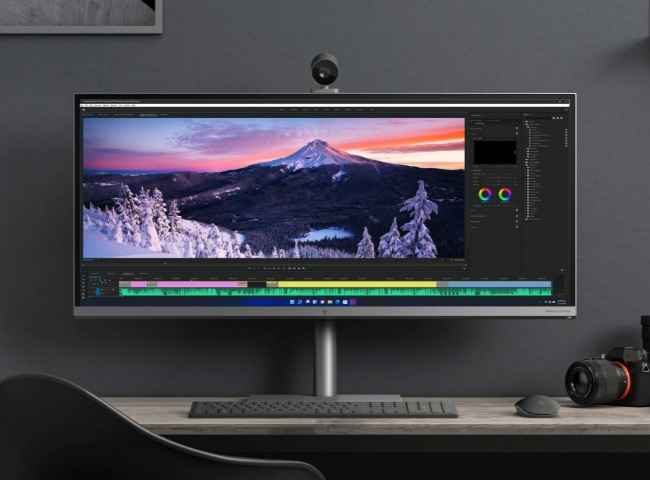
HP upgraded its All-in-One (AiO) series with all new hardware from Intel and Nvidia for the year 2021. The new HP Envy 34-inch AiO desktop PC is an upgrade over the last year’s 32-inch model and therefore features top of the line specs including a 5K display, Intel Core i9 CPU and an RTX 3080.
HP Envy 34-inch All-in-One (AiO) Desktop PC Specifications, Price, Availability in India
The HP Envy 34-inch All-in-One (AiO) PC comes with up to an 11th gen Intel Core i9 octa-core processor for ultrafast computing performance. Furthermore, the HP All in One PC also features up to an Nvidia RTX 3080 GPU, which should be more than enough to play modern games at ultra graphical settings.
In terms of memory and storage, the HP Envy 34-inch All-in-One (AiO) PC comes with upto 128GB DDR4 RAM and 2TB NVMe SSD. Despite being an AiO PC, users can upgrade the 2021 HP Envy desktop thanks to four additional RAM slots and M.2 SSD upgrade slots.
HP Envy 34-inch All-in-One (AiO) PC has a diverse collection of I/O ports including 2X Thunderbolt 4 ports, 1 USB Type C port, 6 USB Type-A ports, and a 3.5mm HDMI out port. HP paired all these components with an Ultrawide 5k (5120x2160 pixels) monitor featuring two internal Bang and Olufsen speakers and a 15W Qi wireless charger.
The HP Envy 34-inch All-in-One (AiO) PC also comes with a detachable 16MP webcam which users can move throughout the length and breadth of the screen. It is a cool concept as people can now place their webcam where it suits them the most. Additionally, the new HP Envy AiO comes with an HP Palette which features a creative toolkit housing several sketches.
In terms of pricing, the HP Envy 34-inch All-in-One (AiO) PC has a price tag of $1,999 or Rs 1,47,000 (approx). It is available in the US through HP’s online store. The HP Envy 34-inch All-in-One (AiO) PC is not available in India however and no official information is available pertaining to its future launch either.
We strongly think that HP should launch the HP Envy 34-inch All-in-One (AiO) PC in India as demand for powerful personal computers is at an all-time high.
Also Read: HP OMEN FanFest 2020: HP Announces Esports Gold Quest Scholarship Worth Rs 12 Lakh
Google is continuously updating Google Workspace regularly, and this time, Gmail for Android is getting an improved search feature. Previously we saw the addition of Chat and Spaces along with the change in the UI as well. This time, Google is adding a search filter, which can be used by tapping the search box and will appear just below it. The aim is to allow users to quickly and easily filter email search results on their mobile devices. It will help you find a specific email or information based on the filter selected from the drop-down list. It will either consist of the name of the sender or the timeframe of receiving the email. You can select a single sender or multiple senders at a time.
Gmail Search Filter Update: Rollout and Availability
Google announced this feature via the Google Workspace Updates blog. This update has begun to roll out from 20th September and will be available to all the users by the end of October. It will be available to all Google Workspace customers, as well as G Suite Basic and Business customers.
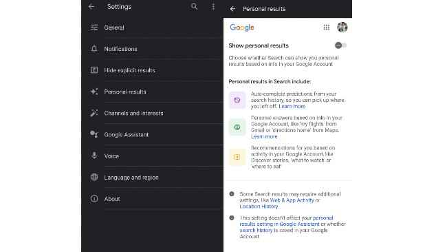
Google Personal results setting for Search on Android
Recently, 9to5Google spotted the addition of Personal results setting on the Google App for Android. This update will be controlling personalised results on Search. Users can turn on or off these settings by following the path Settings > Personal Results on the Google app homepage. It will allow users to disable or enable this option via the app, so you can allow Google to use your account data for personalised results.
This feature will include: Autocomplete predictions based on your search history Results based on your account data like your location, dates and reminders Personalised results based on your regular Google activities like what to eat, places to visit, etc.
Bharat Sanchar Nigam Limited (BSNL) offers a variety of plans that are priced between Rs 300 and Rs 500. These plans come with a good validity period, daily data limit and free SMSs, making them ideal for the masses.
BSNL Rs 499 Recharge (and other plans)
The following are the different BSNL recharge plans priced between Rs 300 and Rs 500, along with their offerings.
Plan
Validity Period
Data
SMS per day
Other offerings
BSNL Rs 499 prepaid plan
90 days
2GB per day
100
Unlimited calls and BSNL tunes, access to the Zing app
BSNL Rs 429 prepaid plan
81 days
1GB per day
100
Unlimited calls, EROS Now streaming
BSNL Rs 447 STV
N/A
100GB high-speed data for 60 days (speed is reduced to 80 Kbps after 60 days)
100
Unlimited calls, EROS Now streaming, BSNL Tunes
BSNL Rs 319 prepaid plan
365 days
2GB daily for 60 days (speed is reduced to 80 Kbps after 60 days)
100
PRBT, unlimited calls
BSNL Rs 398 prepaid plan
30 days validity
N/A
100 for Indian national numbers only
N/A
BSNL also announced a special discount scheme for present landline customers who are migrating to BSNL FTTH, the scheme will facilitate the smooth migration of prepaid DSL connections. According to the reports, the company is offering a discount of Rs 600 to the users who are migrating.
Also Read: BSNL will end all Prepaid Broadband Plans and will migrate existing users to new Postpaid Plan
Bitcoin is the most valuable digital asset but volatile
Bitcoin (CRYPTO: BTC) was created by Satoshi Nakamoto and its ledger started on January 3, 2009. Since its inception, it has become the most valuable and popular digital asset in the world.
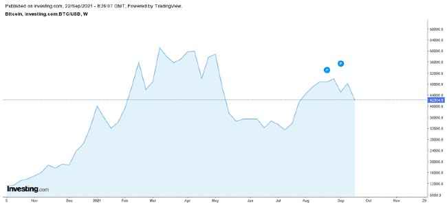
2021 has been a highly volatile year for Bitcoin. In April 2021, it touched an all-time high of $ 65,000 (roughly ₹ 47.7 lakhs). In May 2021, Bitcoin prices corrected by more than 50 percent from the all-time high after Tesla (NASDAQ: TSLA) CEO Elon Musk announced that his company would no longer accept Bitcoin as a payment mode. After a few months of consolidation, it reclaimed the $ 50,000 level (roughly ₹ 36.8 lakhs).
On September 7, 2021, El Salvador became the first country to declare Bitcoin as legal tender.
Bitcoin prices may touch $100K by the end of 2021
According to a report published by Bloomberg, the price of Bitcoin is likely to approach by the end of 2021. “About $40,000 may be the Bitcoin cap a while within that we see as a resting crypto-asset bull market. No. 2 Ethereum is rapidly moving towards No. 1 market-cap status and has been a top driver of the Bloomberg Galaxy Crypto Index in 2021. Bitcoin is more likely to resume appreciating towards $100,000 resistance rather than sustaining below $20,000,” the report read.
On September 16, 2021, Mike McGlone, Bloomberg Intelligence Senior Commodity Strategist, tweeted that he expects a “significant advance in 2021, potentially to $100,00, we believe”.
Can Bitcoin Reach $100,000 in 2021? Five Charts Show Potential - Past #Bitcoin trading trends and the crypto's declining supply vs. mainstream adoption suggest a significant advance in 2021, potentially to $100,000, we believe. pic.twitter.com/0tH7PS7QEI
— Mike McGlone (@mikemcglone11) September 16, 2021 Bitcoin’s supply cap will boost the upside movement
“The human nature of acknowledging a new asset class is what we see as a primary support in 2021,” stated Mike McGlone in Bloomberg Crypto Outlook 2021, June 2021 Edition.
The report states that the supply cap of Bitcoin will help it to become more expensive. Bitcoin supply will keep ‘halving’ every four years, and its supply will stop once its circulation supply touches 21 million coins. “The 2020 halving came amid unprecedented global fiscal and monetary stimulus, along with institutions tilting towards Bitcoin allocations,” the report added.
At the time of writing this article, 1 Bitcoin was trading at $ 42,325.10 (₹ 31,28,438.60).
The smartwatch market is a huge one that’s poised to grow further, so it’s no surprise that more brands want to enter it. Oppo has launched its latest wearable the Oppo Watch Free, which made its debut in China this Saturday and will be available for purchase in India on September 30. It is rumoured to be priced at around Rs. 6,200.
What are the Oppo Watch Free Specifications?
The Oppo Watch Free has a 1.64-inch AMOLED touchscreen with 280x456 pixels resolution and 2.5D curved glass. This smartwatch comes with a 230mAh battery claimed to offer 14 days of battery life in the light battery life mode. It is also claimed to take only 75 minutes to charge fully.
The Oppo Watch Free has more than 100 sports modes including cricket, kayaking, volleyball, rowing, swimming, badminton, skiing, and more. Additionally, it automatically tracks your performance across four sports: walking, running, using the rowing machine, and using the elliptical machine. It also has an e-sports mode that ensures your smartphone’s notifications reach your wearable while you’re gaming (currently, the feature is only available on the Oppo Find X series and Oppo Reno 6 series smartphones).The Oppo Watch Free has a myriad of health features like heart rate monitoring, monitoring your oxygen levels, sleep monitoring, daily activity, and sedentary reminders, and snoring monitoring. The smartwatch is also equipped with a Xiaobu voice assistant.
You can choose from over a 100 watch faces, and even create customised ones that go with your outfit by uploading an image of what you’re wearing. The straps of this smartwatch are made of silicone .It comes with Bluetooth BLE v5 and is compatible with any smartphone that runs at least Android 6.0 or iOS 10.0.
Also Read: Oppo ColorOS 12 based on Android 12 unveiled; list of supported Oppo, OnePlus devices revealed
Poco recently teased the launch of its newest offering in the Poco C series, with the model expected to launch on the 30th of September, at noon. It is believed that this will be the Poco C4 which is the successor to the Poco C3, which was launched last year. The smartphone was Poco’s most affordable model, and was also believed to be a spin off of the Redmi 9C thanks to its triple rear camera and a water drop notch display.
Poco shared an image on its official Twitter account, along with the caption “C U Soon”, which is what led to the speculations of the Poco C4 being launched.
What are the Poco C3 specifications?
The Poco C3 was received well by Indian audiences as it offered decent specifications at an affordable price point. It sold over a million units in January, with the number touching 2 million in February this year.
The Poco C3 has a 6.53-inch HD+ (720x1,600 pixels) display with a 20:9 aspect ratio. The phone has a triple rear camera setup with a 13-megapixel primary sensor at the helm, and a 5-megapixel selfie camera sensor. It runs on an octa-core MediaTek Helio G35 SoC processor, coupled with up to 4GB of RAM. It packs a 5,000mAh battery with 10W charging and carries a Micro-USB port. You can expand the 32GB/ 64GB storage up to 512GB using an SD card.
Poco C3 Price
The Poco C3 is priced at Rs. 7,349 for the 3GB + 32GB model, and Rs. 8,349 for the 4GB + 64Gb model. These prices may go down during the upcoming Flipkart Big Billion Days coming up in October.
Will the new Poco C4 be worth a purchase? Stay tuned for our official review on the same.
Also Read: Interview: Anuj Sharma from POCO India reveals the secret behind the brand’s incredible growth story
Intel’s plans to regain process leadership got a shot in the arm when their new CEO, Pat Gelsinger stepped in and laid down several measures to be implemented. A good chunk of these was unveiled at the Intel Accelerated Event held in July this year. We got to see the roadmap that Intel has laid down for itself to achieve the smallest process node in 2025. The roadmap outlines a very aggressive strategy with rapid jumps from one node to the next one while leveraging some of their existing technologies while also incorporating newer ones. And not only will Intel reap the benefits of the improvements to their process technologies but under their IDM 2.0 strategy, external customers will also get to build their silicon at Intel’s foundries. Let’s take a closer look at Intel’s plans.
Intel Roadmap - Five process nodes in four years
Intel like most of the other silicon manufacturers, such as TSMC and Samsung, has its own naming system. Transistors nodes were named as per the length of the transistor gates in the past but since the transistors have grown smaller, each manufacturer went ahead with their own naming systems. And since there is no industry standard as such, we’re left to simply draw parallels between the process nodes of one manufacturer with that of the other. Intel’s 14nm process was more in line with Samsung and TSMC’s 10nm processes and their newer 10nm Super Fin is close to Samsung and TSMC’s 7nm. At the Intel Accelerated event, Intel went ahead and renamed its existing and upcoming nodes. This includes naming their future nodes using Angstroms instead of Nanometers.
The current node, i.e. 10nm Super Fin (previously considered 10+) will remain as is. However, its successor, the 10nm Enhanced Super Fin (10ESF) will now be referred to as Intel 7. And its 7nm node will be called Intel 4. Similarly, 7+ becomes Intel 3, 5 becomes Intel 20A (A stands for Angstrom). And after 20A comes 18A which is still under development.
From a marketing perspective, this renaming is a huge bonus. Intel’s nodes previously seemed to be catching up even when they had process superiority back in the era of the 22nm and 14nm. This was because the competition process nodes had smaller numbers despite have similar transistor densities. With this new renaming, Intel flips that around and makes it seem like they have process superiority even if the transistor densities would be similar. Here’s a little table to summarise the naming scheme changes.
Old Node Name
New Node Name
Year
Type
10
10
2019
FinFET
10+
10 Super Fin
2020
FinFET
10 Enhanced Super Fin
7
2021
FinFET
7
4
2022
FinFET
7+
3
2023
FinFET
5
20A
2024
Horizontal Nanosheets
5+
18A
2025
Horizontal Nanosheets
We can see that there is a new process node being put into production. Some of the products are already known to us. Alder Lake i.e. Intel 12th Gen Core processors will be the first to be built on the new ‘Intel 7’ node and the same will be used in the Sapphire Rapids products coming to the data centre in 2022. ‘Intel 4’ will be used in Meteor Lake and Granite Rapids, and so on. Each new node will bring with it a lot of improvements and it’s easier to summarise them in a point-wise fashion.
Intel 10 SuperFin (10SF)
Currently used for Tiger Lake, Xe-LP (SG1, DG1), Xe-HPC Ponte Vecchio
Intel 7 (Previously 10 Enhanced SuperFin)
10-15% more performance-per-watt over 10SF
Will be seen in 12th Gen Core Alder Lake (2021) and Sapphire Rapids (2022)
Intel 4
20% more performance-per-watt over ‘Intel 7’
Will see EUV lithography being used
WIll be seen in 13th Gen Core Meteor Lake (2023) and Granite Rapids (2023)
Intel 3
18% more performance-per-watt over ‘Intel 4’
Denser higher-performance library over ‘Intel 4’
Increased use of EUV lithography
Increased intrinsic driver current
Optimised interconnect metal stack
Ready in the latter half of 2023 and used in products in 2024
Intel 20A
Will switch from FinFET to Horizontally Stacked Gate-All-Around Nanosheets (Intel calls these RibbotFETs)
Will introduce a Backside Power Delivery mechanism called PowerVia
Ready in the first half of 2024
Intel 18A
Ready in the first half of 2025
Up until 20A, everything is progressing normally with improvements being made to the way FinFETs are being used in building smaller and denser process nodes. FinFET’s limitations will be realised at that point and the industry as a whole will move towards using Horizontally Stacked Gate-All-Around Nanosheets.
Intel RibbonFET
Every manufacturer likes to call Horizontally Stacked Gate-All-Around Nanosheets using a different term. The industry knows them as GAAFET or Gate-All-Around-FET but Samsung uses the term Multi-Bridge Channel FET or MBCFET whereas TSMC will continue to stick to FinFETs well into their 3nm process so they haven’t revealed what they would be calling it. Intel will use the term RibbonFET. The technology isn’t new. In fact, the first-ever GAA-FET was demonstrated back in 1986. But making GAA-FET small enough and packing them in a dense structure took more than three decades.
RibbonFET uses Ribbon-shaped channels which are surrounded by the gate on all sides, hence, gate-all-around. This enables much better control and helps archive a higher drive current at all voltages. So transistors can switch faster and that inevitably means that performance gets a bump. The following images might help you better understand where the benefits lie.
On the left, we have a typical FinFET design and on the right, you’ve got GAA-FET. In FinFET, you’ve got the gate interfacing with the channels on three sides whereas, with GAA-FET, even the fourth side makes contact with the gate. This results in the higher level of control that we previously mentioned.
The benefits of RibbonFET become more apparent as you scale the designs. With FinFETs, you can scale by increasing the number of fins which inadvertently increases the area used by the transistor. Whereas with RibbonFET, you can add stack another ribbon in the same space and get a higher drive current. Essentially, you can get more done in the same space.
So if processors need to grow smaller and silicon manufacturer’s need to keep Moore’s Law alive, then GAA-FET is the way to go.
Intel PowerVia
Another interesting technology being introduced in the Intel 20A process is Intel PowerVia or what the industry calls Backside Power Delivery. Traditional silicon chip manufacturing consists of layers upon layers of metal and other substances. The communication interface and power supply for these chips are given from the same surface. We’ve seen how a delidded processor looks like, it’s just a package slapped onto a substrate. On the inside of these chips, you’ve got all the different layers. When the power supply comes in from the topmost layer, then by the time it reaches some of the lower layers, it loses out a lot of power because of wire resistances and other parasitic capacitances. The power delivery network has to content for space alongside the signal wires.
This problem is solved by supplying power from the bottom layer and then channelling power to the higher layers using thicker wires or (Through Silicon Via) TSVs. Now chips will have wiring on both sides with signal wires on one end and power wires on the other. The transistors will get sandwiched between these two layers.
With PowerVia, you no longer have the Power Delivery Network (PDN) contending with the signal wires for space. Nor is it that big a source for interference anymore. This leaves room for the signal wires to be better optimised.
To get more information on RibbonFET, PowerVIA and Intel’s aggressive growth plans, we reached out to Intel with a few queries. Deemanth Nagaraj, Intel Fellow was more than accommodating while answering our queries. Here’s what Intel had to say.
Digit - What are the challenges that PowerVia is meant to resolve? Is it explicitly linked to RibbonFET or are the two independent of each other?
Intel - PowerVia will be an industry-first deployment of a backside power delivery network technology when it is introduced with Intel20A. It significantly reduces the need for power routing on the front side of the wafer by bringing power in from the backside, making more resources available for optimizing signal routing and as a result, reducing signal delays. The overall result is a performance boost at the IP block level and a reduction in power leakage.
PowerVia is independent of RibbonFET, which is Intel’s implementation of the Gate All Around transistor. We expect to test PowerVia on earlier nodes to ensure this groundbreaking technology is fully ready before it ramps in volume with Intel 20A in 2024. We also expect first product for PowerVia to be a leadership client solution.
Digit - ASML announced a delay of 3 years (https://ift.tt/3ijkZ0o) for their High-NA machines to hit production. Will that affect Intel's 20A or 18A plans?
Intel - We can’t comment on speculative reports. We can say that Intel is positioned to receive the first High NA EUV tool in the industry, and we are driving to enable its introduction in 2025. We have a very strong partnership with EUV equipment leader ASML, and our plans to stay on the leading edge of EUV usage are well underway.
Digit - The plans to return to process leadership seems to be quite aggressive. On top of that, you're also reducing the cadence cycle and going back to tick-tock. Isn't it an extremely risky move if you wish to release client products on newer nodes every year? Or would we see fewer client launches to allow for more time to iron out each node?
Intel - Intel continues to compete and win in our core PC market with a steady drumbeat of highly competitive CPU and platform innovation. We are laser focused on delivering a predictable yearly cadence of innovation and are well on the path to get back to our “tick tock” momentum.
The roadmap we’ve shown at Intel Accelerated is one of the most detailed roadmaps we’ve ever provided for process and packaging technologies and it shows a better than yearly cadence: 5 process nodes in 4 years! We have funded the R&D and capital for the teams and are taking all the right steps to ensure we execute at this incredible pace.
Digit - Continuing with the previous question, what kind of risk mitigation strategies (backporting?) are you implementing to ensure that your launch cycles are on schedule?
Intel - We are embracing the industry as never before in areas like equipment, EDA and research:
• We’re collaborating across our equipment suppliers to make sure we are leveraging the best from the industry. This includes a deep partnership with ASML on EUV, both in fully embracing EUV for Intel 4 and staying on the leading edge of EUV with our swift adoption of High-NA, the next major technology change on the EUV roadmap.
• We’re adopting industry-standard approaches where it makes sense, like industry-standard EDA tools and models.
• We’re building on our partnerships with leading research organizations, such as IBM, IMEC and Leti. This combined with our own components research gives us confidence that we are on very solid footing.
The ecosystem support we’ve demonstrated shows the confidence our customers and partners have on the predictable cadence that Intel is now on – including deep technical validation from customers, like the announcement with Qualcomm.
Digit - How are thermals being managed on chips using Backside Power Delivery? Is it more of an offset because the node becomes more efficient, or do you have to make changes with the way you package the chip for production?
Intel - Thermal management is a key element in all packaging configurations and is determined based on a number of inputs – die floorplan, interconnect architecture, die thickness, package configuration, to name a few – and PowerVia power delivery is one of those elements that is input into the thermal design point (TDP) calculation. Thermal solutions are ultimately determined by the best combination of thermal interface materials and system cooling solutions that meet the customer’s need. Our assembly technology is designed to be flexible so that our customers can optimize their products to manage TDP, footprint and cost. This is a key element of our IDM 2.0 strategy and one reason why we believe we have an advantage over the competition in packaging.