Intel opened up about their technology roadmaps across all of their hardware and software verticals at Intel Architecture Day 2020. Like with the previous Architecture Day that was held in 2018, Intel focused on 6 key aspects which they call the “Six Technology Pillars” and they are: Process and Packaging, XPU Architecture, Memory, Interconnect, Security and Software. Intel unveiled plenty of information regarding their upcoming CPU cores, process technology improvements, all the different architecture variants for the Xe GPUs, memory advancements with Optane Persistent Memory and their efforts on the software front through the OneAPI program. Here’s a brief overview of everything that went down at Intel Architecture Day 2020.
Process and PackagingIt’s no secret that Intel took on a rather ambitious project with their 10nm and 7nm process nodes and in doing so, they’ve had to experiment a lot with the transistor process, lithography and material technology that went into each of their upcoming process nodes. Intel stated that they were moving away from the silliness of tacking on additional plusses (14nm++++) each time an improvement was made to the process technology. Instead, they will now be using more descriptive terms and letting the world know more about the improvements made. Superfin, is the first step in this new “descriptive” direction. Intel’s upcoming 10nm process will now be referred to as Intel 10nm Superfin.

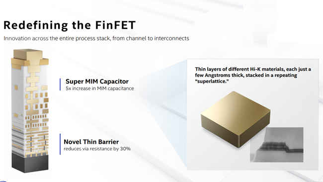
Key improvements include improving the transistor gate pitch to allow higher drive current, enhanced epitaxial source/drain to reduce resistance and lower strain over time, lastly, the gate process has also been improved to help with channel mobility. At a macro level, they’ve introduced the Super MIM Capacitor which is basically a stacked lattice of thin layers of different Hi-K materials, each of which is just a few angstroms thick. An angstrom is one hundred-millionth of a centimeter. Simply by using different Hi-K materials they build a capacitor and the stacking helps increase the capacitance of the entire structure. Another improvement is with the reduced resistance of the vias within the stack.
All of the above improvements had to do with the individual chips. Zooming out to an even larger scale lies the challenge of interconnectors for bridging chips together. Intel makes use of several types of interconnects to enable this. The most recent of which is Foveros which helped make their latest Lakefield CPUs happen. Lakefield interconnects had a bump pitch of between 50-25 microns and their future interconnects are expected to have a bump pitch of less than 10 microns. They’ve also taped out chips using hybrid interconnects which make use of multiple interconnect technologies such as Co-EMIB and ODI(Omni-Directional Interconnect). Each of these interconnects are suitable for a different use case. Some work with enabling the stacking of a smaller package onto a large package whereas other interconnects help with the situation with a larger package being stacked onto a smaller one. All of these improvements will help Intel integrate more chiplets within a smaller footprint.
XPU Heterogeneous Architecture and Tiger LakeThe impact of a CPU microarchitecture is dependent on its generality i.e. how many different applications can you execute using a particular architecture. Intel has a diverse portfolio of silicon which is spread across CPUs, GPUs, AI accelerators and FPGAs. Each of these adhere to a particular architecture domain. CPUs are scalar, GPUs are vector, AI accelerators are Matrix and FPGAs are spatial. These are all defined on the basis of their typical workloads. For example, CPUs are generic, GPUs are highly parallelised, AI accelerators have to handle a lot of matrix match and FPGAs are used for more cutting edge algorithms that the other domains aren’t as good at handling.
Intel then moved into stating their goals for Tiger Lake, their upcoming processor family. To summarise, Intel wanted a generational leap in performance with disruptive graphics, scalable AI, increased memory bandwidth and ensure data security. We’ve already covered the packaging and process aspect. Coming to the performance factor, Tiger Lake will be using Willow Cover which is built upon their Sunny Cove cores that have been redesigned to have a larger non-inclusive cache and with security improvements to protect against return or jump oriented attacks. Intel states that they have achieved large frequency gains while maintaining power efficiency. The net result being that they have a greater dynamic V-F curve to play with.

For graphics, Intel had already demonstrated the “Horseshoe Bend” concept earlier this year at CES 2020 which had Xe Graphics. Since Xe is a broad architecture, Intel has different architecture variants for each focus area. With CPUs, they’re using Xe-LP architecture and in Tiger Lake, we can expect up to 96 Execution Units with 3.8 MB of L3 cache.
Tiger Lake will support LP4x-4267 and DDR4-3200 memory and up to LP5-5400 memory for when we have commercial kits available. Overall, the total memory bandwidth would be about 86 GB/s and Tiger Lake will have two memory controllers on the package.
Since Willow Cove builds upon Sunny Cove, we have AI capabilities built in as well. Intel calls this the Gaussian and Neural Accelerator (GNA 2.0). The key improvement here is that it is optimised for low-power neural inference and also consumes less CPU compute resources.
from Latest Technology News https://ift.tt/3gVB0Gj

No comments:
Post a Comment